Power
The nRF9151 Micro Breakout DevKit2 provides a flexible power arrangement for the three power domains VDD, VDD_GPIO and VDD_GPS.
The USB-C port provides 5V power to a linear regulator outputting 3.3V. By default all three nRF9151 Micro Breakout power domains are powered by 3.3V via pre-made solder bridges JP8, JP10 and JP12.
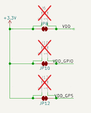
To test the Micro Breakout with an alternative voltage, break the respective solder bridge and apply power to the header pads.
The following scenarios are possible.
Measure VDD current
- Break solder bridge
JP8by scraping away the pre-made connection - Apply a current probe between pins 1 & 2 of
J6
Supply GPIO with 1.8V
- Break solder bridge
JP10 - Apply a custom voltage to pin 1 of
J10
It may also be necessary to remove JP13 through JP19 to disconnect the 3.3V powered on-board peripherals.
Power the GPS LNA from 5V
- Break solder bridge
JP12 - Attach pin 1 of
J12to a 5V output on the double-socket headers
Check the maximum Supply Voltage specifications for the VDD_GPS pin.