Usage
The nRF9151 Micro Breakout is a minimal wrapper around the Nordic nRF9151 SiP, providing all essential circuitry from Nordic's reference designs for correct operation — including decoupling and ENABLE pin pull-up. All 32 nRF9151 GPIO are exposed on the castellated edge pins.
Unlike other nRF9151 development kits, the Micro Breakout does not restrict specific pins to specific functions. Many kits bundle flash memory or an accelerometer, forcing the use of certain GPIO for SPI and/or I2C and constraining the user's application. The Micro Breakout imposes no such constraints.
The Micro Breakout is designed to be as small as possible, giving users a complete, tested nRF9151 RF design without requiring large carrier boards.
Architecture
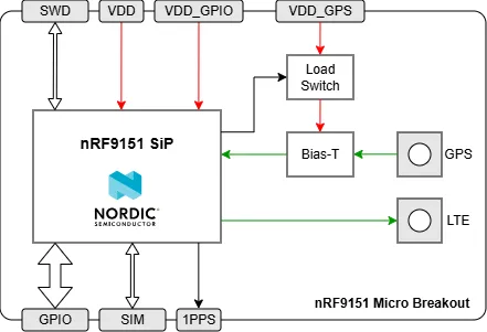
All nRF9151 SiP GPIO pins are attached to the castellated edges in sequential order. The four UICC/SIM pins arrive uninterrupted at the breakout edge. Power is provided via the VDD* pins with the relevant conditioning (bypass capacitors and filters) on-board. The LTE and GPS signals are presented via compact U.FL RF connectors for direct antenna or pigtail connections. The Micro Breakout can control power to a GPS LNA via an integrated Power Switch and Bias-T. SWD programming signals connect directly to the nRF9151 SiP.
Pinout
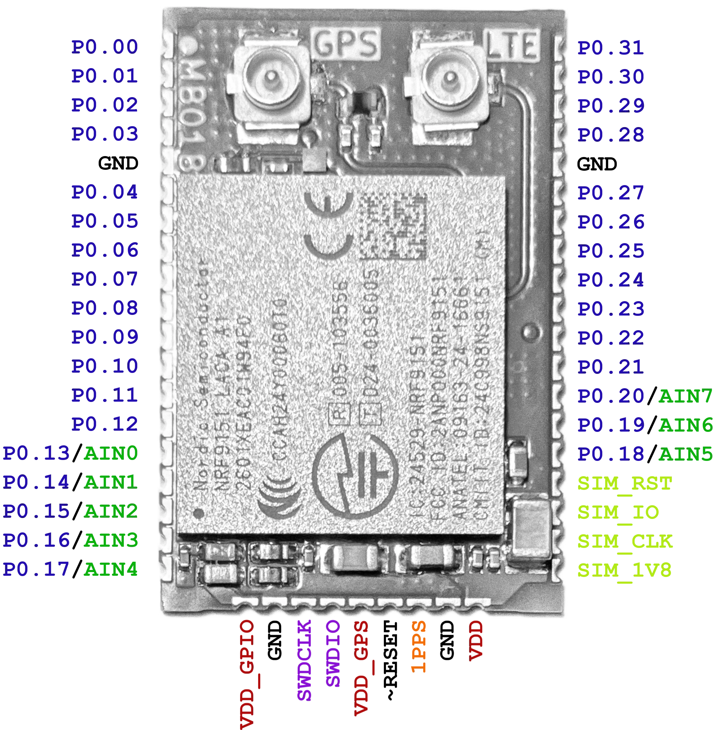
The Micro Breakout uses a 3-side castellated edge design to expose all 32 GPIO and required pins with only a small increase over the base nRF9151 SiP footprint. The fourth side (top, near the U.FL connectors) has no castellated pins to minimise routing near the RF connectors.
GPIO pins are broken out sequentially anti-clockwise from top-left (P0.00) to top-right (P0.31). With U.FL connectors at the top:
- Left — GPIO only,
P0.00throughP0.17 - Bottom — Power, SWD, GND, PPS, Reset
- Right — UICC/SIM and remaining GPIO,
P0.18throughP0.31
GPIO pins P0.13 through P0.20 may be used as analogue inputs AIN0 through AIN7 as per the Nordic docs.
Power
The nRF9151 SiP requires two power supplies:
- VDD — supplies the nRF9151 core CPU and modem via an internal voltage regulator
- VDD_GPIO — supplies the 32 GPIO pins
The Micro Breakout exposes a third supply:
- VDD_GPS — provides power via the Power Switch to an LNA embedded in the GPS antenna
Four GND pins are exposed and shared across all three VDD* power domains. These should be connected via a low-impedance trace to the carrier board ground.
The recommended and absolute maximum ratings for the power pins are given in Supply Voltage.
GPS
Overview
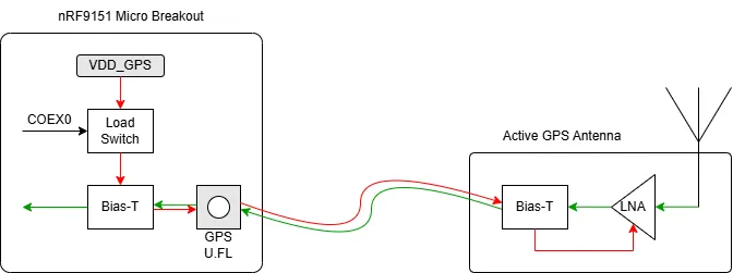
GPS signals at ground level are extremely weak, requiring a Low Noise Amplifier (LNA) close to the GPS antenna. Most GPS antennas are active — they embed an LNA with the antenna. A passive GPS antenna does not. Where an active antenna is used, the receiver supplies DC power to the LNA over the same coaxial cable carrying the GPS signal, using a Bias-T arrangement that prevents the DC from interfering with the RF signal. This allows the GPS antenna to be placed many metres from the receiver without signal loss.
The Micro Breakout presents a single U.FL connector for GPS and assumes an active (LNA-embedded) external antenna. Unlike many GPS-specific devices (e.g. u-blox), the nRF9151 SiP cannot supply DC power to the antenna directly — the Micro Breakout provides this capability instead.
A user-defined voltage is supplied to the GPS LNA via the VDD_GPS pin. As per the Supply Voltage specifications, this can range from 1.1 V to 5.5 V. The voltage at VDD_GPS is not used for any other circuitry on the Micro Breakout.
If GPS is not required, VDD_GPS may be left floating. If powering the GPS antenna separately, leave VDD_GPS floating and ensure the Power Switch is never enabled.
Power Switch control
When VDD_GPS is supplied, the Power Switch must be enabled to pass power to the GPS antenna. The control signal is the active-high COEX0 pin on the nRF9151 SiP. Full documentation is in the Nordic docs.
COEX0 pin state:
- High — Power Switch enabled;
VDD_GPSis applied to the GPS antenna - Low — Power Switch disabled;
VDD_GPSis disconnected from the GPS antenna
See AT commands for COEX0 for software configuration.
PPS
A one pulse per second (PPS) signal is a digital pulse with a period of precisely one second, where the rising or falling edge marks the start of that second. Dedicated GPS receivers commonly output a PPS signal to allow downstream equipment to align time-of-day data (from NMEA) with precise second ticks.
The nRF9151 SiP includes a GPS & QZSS receiver which can output a PPS signal from the COEX1 pin, aligned to UTC. The duty cycle is configurable via modem commands.
The Micro Breakout exposes COEX1 as the 1PPS edge connector. When GPS is active and COEX1 is configured in firmware, this pin emits a UTC-aligned 1 PPS signal.
PPS accuracy
The nRF9151 SiP is not a dedicated GNSS timing solution. The 1PPS accuracy is at best ±35 ns and will vary with GPS signal quality.
Connectors
The LTE and GPS signals are exposed via two U.FL connectors. These are excellent for compact designs but are not rated for repeated mating. U.FL connectors are rated for no more than 30 mating cycles.
- U.FL PCB connectors are male.
- A U.FL to SMA pigtail is recommended to avoid excessive mating cycles.
- Take care when removing U.FL connectors to avoid PCB damage.
- Do not use excessive force when inserting U.FL cables.
- Cable restraint or adhesive may be required in high-vibration environments — avoid contact with RF traces.
Reset
The ~RESET pin is connected to the nRF9151 SiP via a 1 kΩ series resistor and 100 nF capacitor to GND, as per Nordic documentation. The pin is active low and does not require an external pull-up.
ESD
The Micro Breakout provides no ESD protection beyond the 1.5 kV HBM level built into the nRF9151 SiP itself. This applies to all GPIO, SIM, and antenna connections. Depending on the application, additional ESD protection on the carrier board may be advisable for exposed pins.
Use ESD mats and wrist straps when handling the board manually to avoid permanent damage to the nRF9151 SiP.