DevKit2 — Overview & Specs
The DevKit2 is a full development kit built around the nRF9151 Micro Breakout, providing everything needed to start developing LTE-M and NB-IoT applications.
nRF9151 Micro Breakout included
The nRF9151 Micro Breakout DevKit2 is supplied with a single nRF9151 Micro Breakout attached. An nRF9151 Micro Breakout does not need to be purchased separately.
Key Features
- Exposes all Micro Breakout pins to 2.54mm double sockets
- USB-C for UART connection to nRF9151 SiP
- JEDEC-compatible 64Mbit flash over SPI
- I2C temperature sensor for testing data logging applications
- Three user LEDs and a GPS Pulse Per Second (PPS) LED
- General purpose user button and reset button
- Nano SIM (4FF) card slot
- Removable solder bridges for user-defined reconfiguration of DevKit2
- SWD programming available via Pogo pins and standard 10-way Samtec FTSH header
- Headers available for individual Micro Breakout power domain current measurement or separate supply
Architecture
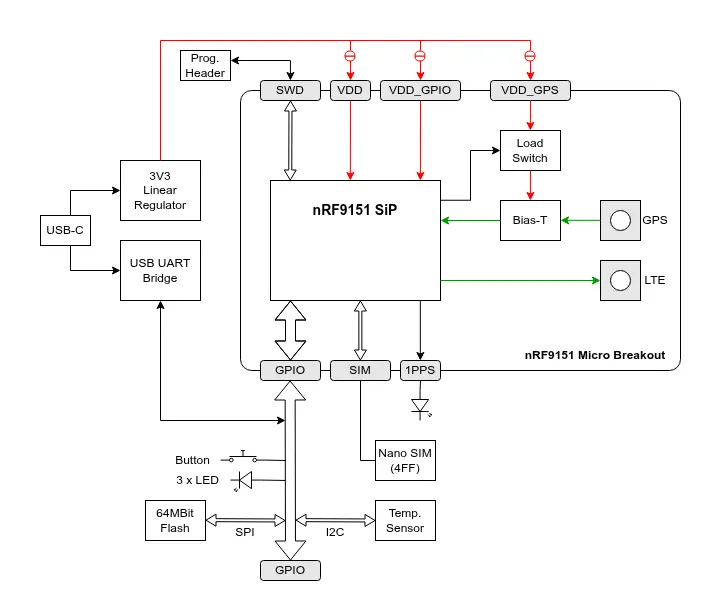
The DevKit2 breaks out all GPIO pins to double-gang 2.54mm sockets, plus extra GND, 5V and 3.3V power. The USB-C port connects to a UART bridge and provides 5V power, and 3.3V via a linear regulator. By default all three Micro Breakout power domains (VDD, VDD_GPIO and VDD_GPS) are powered from 3.3V, unless the solder bridges are broken and power routed differently. Certain GPIO pins drive three LEDs and one button. Likewise, a TMP1075D temperature sensor and MX25R6435F 64Mbit flash are connected to GPIO pins set as I2C and SPI. All of these GPIO can be disconnected from their default functions via solder bridges. The 1PPS output from COEX1 is presented via a single LED and pad. A key feature of the DevKit2 is the ability to disconnect the default functions via solder bridges and route the board exactly as required.
Schematic
The full DevKit2 schematic is available as a PDF, covering the power domains, solder bridge connections, on-board peripherals and programming header. It is the definitive reference when reconfiguring the board or designing against it.
Solder bridges
The DevKit2 uses 19 solder bridges labelled JP*, all on the bottom of the board. These are connected by default, but may be disconnected by scraping the trace between the two bridge points. If the connection needs to be remade later, a solder bridge can be applied across the two pads.
The list of solder bridges and their function is given below:
JP* |
Default | Function |
|---|---|---|
JP1 |
Connected | Connects the 1PPS output from the nRF9151 (COEX1) to the PPS LED. The PPS pad is always connected. |
JP2 |
Connected | Enables the 5V LED. Remove this link to disable 5V power indication. |
JP3 |
Connected | Enables the 3.3V LED. Remove this link to disable 3.3V power indication. |
JP4 |
Connected | Connects P0.00 to the user button BTN. |
JP5 |
Connected | Connects P0.29 to LED1. |
JP6 |
Connected | Connects P0.30 to LED2. |
JP7 |
Connected | Connects P0.31 to LED3. |
JP8 |
Connected | Connects VDD to 3.3V power. Remove this connection for current measurement or alternative voltage supply. |
JP9 |
Connected | Connects P0.11 to FTDI transmit — P0.11 should be set as UART receive in the device tree. |
JP10 |
Connected | Connects VDD_GPIO to 3.3V power. Remove this connection for current measurement or alternative voltage supply. |
JP11 |
Connected | Connects P0.12 to FTDI receive — P0.12 should be set as UART transmit in the device tree. |
JP12 |
Connected | Connects VDD_GPS to 3.3V power. Remove this connection for current measurement or alternative voltage supply. |
JP13 |
Connected | Connects P0.21 to chip select (MEM_~CS) on MX25R6435F 64Mbit SPI flash. |
JP14 |
Connected | Connects P0.25 to CLK on MX25R6435F 64Mbit SPI flash. |
JP15 |
Connected | Connects P0.26 to MOSI on MX25R6435F 64Mbit SPI flash. |
JP16 |
Connected | Connects P0.22 to MISO on MX25R6435F 64Mbit SPI flash. |
JP17 |
Connected | Connects P0.04 to SDA on TMP1075D I2C. |
JP18 |
Connected | Connects P0.05 to SCL on TMP1075D I2C. |
JP19 |
Connected | Connects P0.06 to TMP1075D alert pin. |
Temperature sensor
The DevKit2 includes a TMP1075D temperature sensor with a typical accuracy of ±0.25 °C and ultra-low power consumption. It connects to the nRF9151 Micro Breakout over I2C using default pins P0.04 (SDA), P0.05 (SCL) and P0.06 (Alert). Zephyr provides a driver for the TMP1075D, making integration into software projects straightforward.
64Mbit flash
The DevKit2 includes a Macronix MX25R6435F 64Mbit flash connected over SPI using GPIO P0.26 (MOSI), P0.22 (MISO), P0.25 (CLK) and P0.21 (chip select). If the flash chip is not required, these pins can be disconnected from the GPIO using solder bridges. The flash device is accessible from Zephyr using the standard jedec,spi-nor driver.
Debug Interface
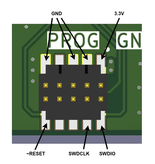
SWD programming is available via a standard 10-way Samtec FTSH header and a labelled single row of 2.54mm-pitch holes.
SIM card
The DevKit2 supports a nano SIM (4FF) via the SIM card holder. A SIM card must be present before any network connection can occur.
Electrostatic Discharge
The DevKit2 provides no ESD protection beyond the human body model level built into the nRF9151 SiP. See ESD on the Micro Breakout for details.